

")


")
Altera Cyclone II EP2C5T144 FPGA Dev Board
£18.99
VAT included
This development board is a low cost way to get into the world of FPGAs and programmable logic. Based on a 144 pin Altera Cyclone II (EP2C5ST144C8N) device this board is a significant step up from our popular MAX II CPLD development board (HCDVBD0006). It features standard 0.1" pitch breakout headers for the devices 89 usable I/O cells, on-board...
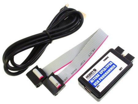
This development board is a low cost way to get into the world of FPGAs and programmable logic. Based on a 144 pin Altera Cyclone II (EP2C5ST144C8N) device this board is a significant step up from our popular MAX II CPLD development board (HCDVBD0006). It features standard 0.1" pitch breakout headers for the devices 89 usable I/O cells, on-board 50MHz crystal oscillator which provides the FPGA's internal clock source, on-board 3.3V & 1.2V regulators with 2.1mm DC power socket, user LED's and both JTAG and ASP with EPCS device programming headers which are directly compatible with our Altera USB programmer (see item HCDVBD0007). 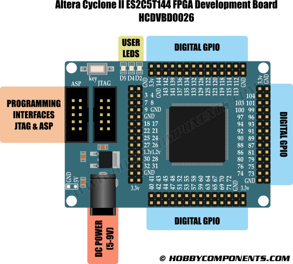
Board Features:
Breakout headers for all usable I/O
On-board 3.3V & 1.2V regulators.
Single 5V power source via 2.1mm DC socket
3x programmable user LEDS connected to pins 3, 7 & 9
Power LED
On-board 50MHz oscillator connected to pin 17
Reset button
JTAG interface
ASP serial programming interface with on board EPCS4 storage
Compatible with the Altera Quartus 2 and free web edition software
FPGA Features:
Number of Logic Elements: 4608 (16 LE's per block)
Number of 4K bit memory blocks: 26 (119,808 total bits)
Number of embeded multipliers: 13 (can be configured as 2 x 9 bit or 1 x 18 bit)
Number of PLL's: 2
Maxium usable IO: 89
Please note: Depending on your design, FPGAs can consume a large amount of power. If you have a complex design it may exceed the capabilities of the on-board regulators. In this case you should power the development board via the power header pins.
Datasheet and software tools available on our support forum here.
HCDVBD0026
Specific References
2 other products in the category
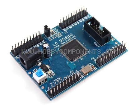

This development board is a low cost way to get into the world of FPGAs and programmable logic. Based on a 144 pin Altera Cyclone II (EP2C5ST144C8N) device this board is a significant step up from our popular MAX II CPLD development board (HCDVBD0006). It features standard 0.1" pitch breakout headers for the devices 89 usable I/O cells, on-board...